A Simple Circuit Implementation
of a Van der Pol Oscillator
Ned J. Corron
In the study of nonlinear dynamics and applied mathematics, the Van der Pol oscillator is commonly used to illustrate various phenomena including stability, Hopf bifurcation, limit cycles, and relaxation oscillations. This mathematical model was originally developed for an electronic oscillator built using vacuum tubes; however, it is difficult today to realize this circuit in its original form due to the replacement of tubes with semiconductor technology. Thus, it is particularly instructive to have a modern circuit implementation for demonstrating these mathematical concepts in a physical device.
Mathematically, a general form of a Van der Pol oscillator is
![]() (1)
(1)
where e and a are constants, u(t) is the dependent state that depends on time t, and a dot denotes differentiation with respect to time. Equivalently, the oscillator (1) can be written in system form as
![]() (2)
(2)
where ![]() and
and ![]() . This latter form is
convenient for directly interpreting the response of the system in x‑y phase space.
. This latter form is
convenient for directly interpreting the response of the system in x‑y phase space.
The oscillator (1) is widely used to demonstrate nonlinear dynamics since it is amenable to analysis. Specifically, asymptotic techniques can be applied for the cases of both small and large e to predict the amplitude response and waveform shape. For small e, it is a standard exercise to show that u = 0 is stable for a < 0; a Hopf bifurcation occurs at a = 0; and a stable limit cycle exists for a > 0, for which
![]() (3)
(3)
where f is an arbitrary phase. For large e, the oscillator produces relaxation oscillations, which approach a square wave. Numerical simulations can be used to examine the continuum that bridges these limits.
The electronic circuit shown in Figure 1 is a Van der Pol oscillator; that is, the circuit is appropriately modeled by equation (1), or equivalently by the system (2). The voltages Vx and Vy correspond to the states x and y, respectively. In the circuit, the amplifiers U1, U2, and U3 are any standard operational amplifiers, such as TL082. The devices U4 and U5 are AD633 integrated circuits, which are low cost analog multipliers with differential inputs and divide-by-ten output. Specific component values are suggested in Table 1.
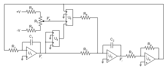
Figure 1. Circuit for a Van der Pol oscillator.
|
Component |
Value or Device |
|
R1,
R2, R3, R4 |
10 kW |
|
R5,
R6 |
470 kW |
|
R7 |
100 kW potentiometer |
|
R8 |
1 kW (see text) |
|
C1,
C2 |
0.01 mF |
|
U1,
U2, U3 |
TL082, ½ Dual BiFET Op Amp |
|
U4,
U5 |
AD633, Low Cost Analog Multiplier |
Table 1. Suggested component values and devices.
For the component values suggested in Table 1, the parameter e is set to 0.1; however, other values for e can be selected by changing R8, where
![]() . (4)
. (4)
The parameter a is set by adjusting the voltage divider at R7, where
![]() . (5)
. (5)
Including R5 and R6 in the voltage divider roughly compensates for the factor of 10 in (5), thereby providing the useful range -15 < a < 15 using a ±15-volt power source. The frequency at the Hopf bifurcation is
![]() (6)
(6)
which can be adjusted by changing both C1 and C2 together. In operation, the voltage Va is monitored using a digital voltmeter, and the voltages Vx and Vy are observed with an oscilloscope.
|
a = -0.02 a = 1.43 a = 3.69 a = 7.39 a = 13.2 Figure 2. Observed response viewed in the x‑y phase plane for the Van der Pol circuit with various values of the control parameter a. |
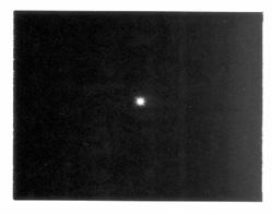
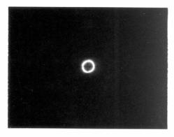
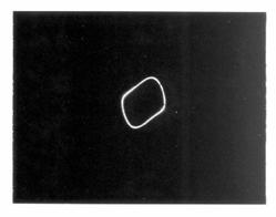
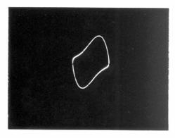
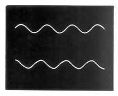
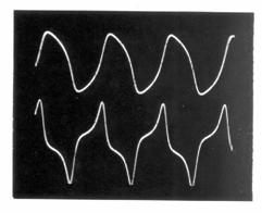
The interesting nonlinear dynamics of the Van der Pol oscillator can be observed by scanning Va from negative to positive values. In Figure 2, the system phase space trajectory observed for various Va are shown. These figures are screen snapshots taken from an analog oscilloscope configured in an x-y mode, with Vx and Vy connected to the x and y channels, respectively. In a phase plane picture, a closed path represents a periodic waveform, and the special case of a sinusoidal waveform displays as a circular or elliptical path. Deviation from an elliptical orbit indicates the presence of harmonics, and the waveform is no longer a pure sinusoid. With a negative Va, it is seen that the steady state Vx = Vy = 0 is observed, thus indicating it is stable. As Va increases toward zero, it is seen that this steady state becomes more noisy. This is a precursor for the impending loss of stability of the steady state that will occur at the Hopf bifurcation. As Va is increased just past zero, a Hopf bifurcation is observed, in which a small amplitude limit cycle emerges from the steady state. These initial oscillations are almost perfect sine waves in both x and y, seen as a circle in the phase space and the oscilloscope display. As Va increases from zero, the amplitude of the sinusoidal oscillations quickly grows, confirming the quadratic amplitude response in (3). However, this rapid growth abates as Va gets larger. Eventually, the waveform begins to distort from sinusoidal as the nonlinear characteristics of the circuit begin to dominate. At this point, the circuit begins to function as a relaxation oscillator, generating a waveform characterized by rapid switching between two metastable states. In Figure 3, actual time traces of the waveforms for both Vx and Vy are shown for two positive values of Va. By comparing the traces in Figure 3, it is seen how the waveform deviates from sinusoidal for larger Va.
|
a = 1.43 a = 13.2 Figure 3. Observed x (top) and y (bottom) time traces for the Van der Pol circuit with two values of the control parameter a. |
The response described by (3) can be confirmed experimentally using the circuit. In Figure 4, the theoretical and observed amplitude responses for the oscillator are plotted as a function of the control parameter a. In this figure, two observed responses are shown. These responses are derived from the peak-to-peak voltage observed for the voltages Vx and Vy. For small a > 0, the responses for both voltages are virtually identical and agree with that predicted in (3). However, for larger a, the two observed responses differ significantly due to the waveform deviation from sinusoidal. It is interesting to note that the response observed for Vx continues to track the prediction (3) even though the assumption of weak dissipation is no longer valid.
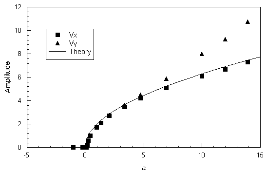
Figure 4. Observed amplitude response for the Van der Pol circuit as a function of the control parameter a.
In conclusion, this brief tutorial presents a modern Van der Pol circuit that is capable of showing various nonlinear phenomena including stability, Hopf bifurcation, limit cycles, and relaxation oscillations. As a result, this simple experimental system provides a useful tool for exploring important concepts in nonlinear dynamics and serves as a starting point for further investigations in nonlinear and chaotic systems.

